Learn more about our antenna simulation software…
Introduction
This example demonstrates the performance of an antenna array for 140 GHz wireless communication purposes, such as for use in a 6G application. The base element design consists of a TE 340-mode substrate-integrated cavity (SIC) excited 2x2 slot antenna subarray in low-temperature co-fired ceramic (LTCC). The base elements are combined to make an 8x8 array with a wide bandwidth from 130 to 145 GHz, a peak gain of 20.5 dBi, stable radiation patterns over the frequency range, efficiency around 60%, small size, and simplified construction. The simulations are performed in XFdtd EM Simulation Software and are based on the original antenna design presented in (1).
Device Design and Simulation
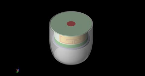
The antenna array is comprised of 8x8 elements connected by two types of H-junction substrate integrated power dividers. Each single element (shown in Figure 1) has four metal layers separated by LTCC substrate layers of Ferro A6M with dielectric constant 5.9 and loss tangent 0.002. The top layer has two TE 210-mode substrate integrated cavities (SIC) which are defined by vias visible on the top metal layer in Figure 1 and in Figure 2. Figure 2 also shows the second metal layer with four radiating slots. Metal layer 3 is shown in Figure 3 with the vias defining the SIC feeding the four slots of Figure 2 along with two matching posts in the center of the cavity. In the center of metal layer 3 is a slot from the lower feed layer. The lower layer is shown in Figure 4, where the vias define the substrate integrated waveguide (SIW) of the feed. The single matching post in the SIW is also visible as well as a waveguide feed applied to the opening in XFdtd.
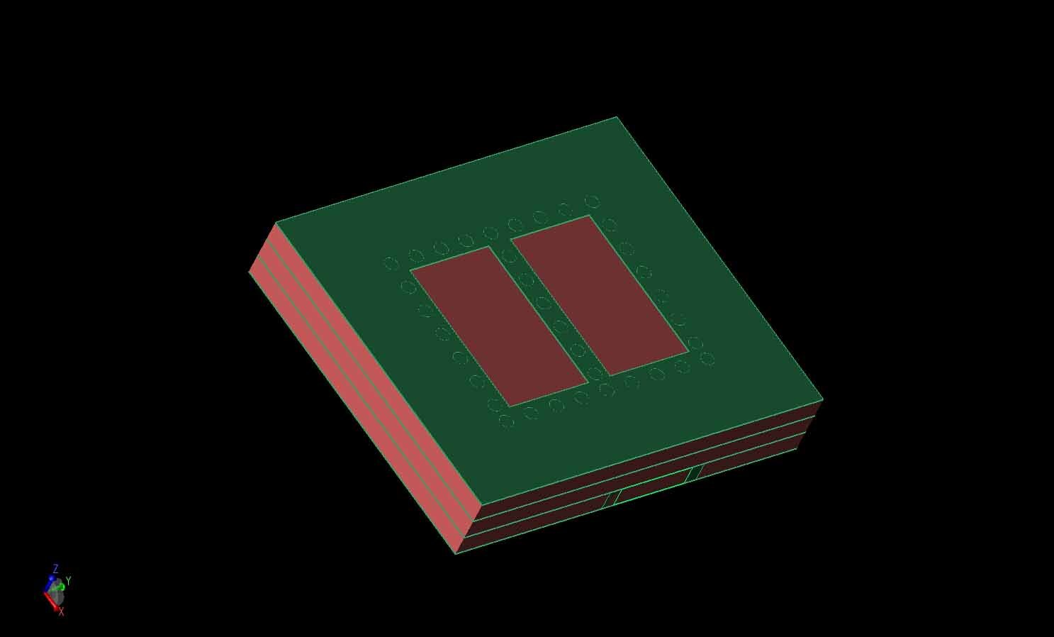
Figure 1: A three-dimensional CAD rendering of the SIC excited 2x2 antenna element is shown with metal layers in green and LTCC layers in red.
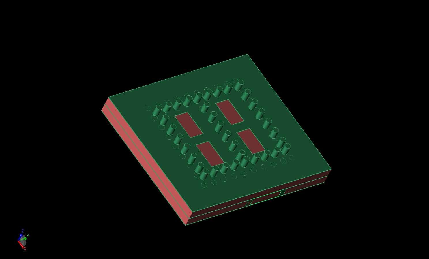
Figure 2: The top layer cavity of the antenna element is shown with the four radiating elements in metal layer #2 feeding into the TE210 mode substrate integrated cavities.
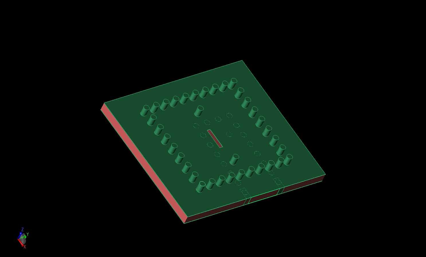
Figure 3: The TE340 mode SIC above metal layer #3 is shown with the feeding slot in the center and the two matching posts above and below the slot.
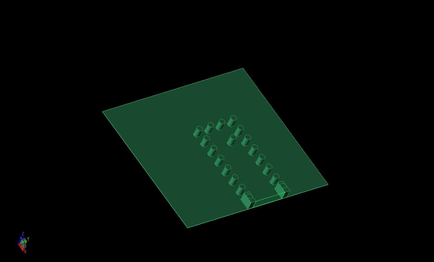
Figure 4: The input is fed into the antenna through a feed layer above metal layer #4, which contains a SIW region and a matching post below the feed slot of metal layer #3 (not shown).
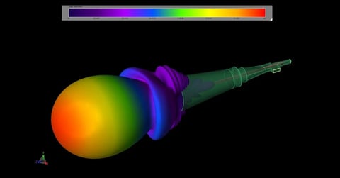
Following the EM simulation, the resulting return loss shown in Figure 5 demonstrates a -10 dB bandwidth for the single element from 131.63 to 146.45 GHz. The gain at a point above the element is plotted versus frequency in Figure 6 and shows values from 9 to 11.5 dBi over the bandwidth of the antenna. In Figure 7 the gain patterns in the two principal planes are shown at 131 GHz with broad beamwidth. Similar gain pattern results are shown in Figure 8 for 135 GHz, in Figure 9 for 140 GHz, and in Figure 10 for 147 GHz. These plots demonstrate the stability of the patterns over a wide frequency range.
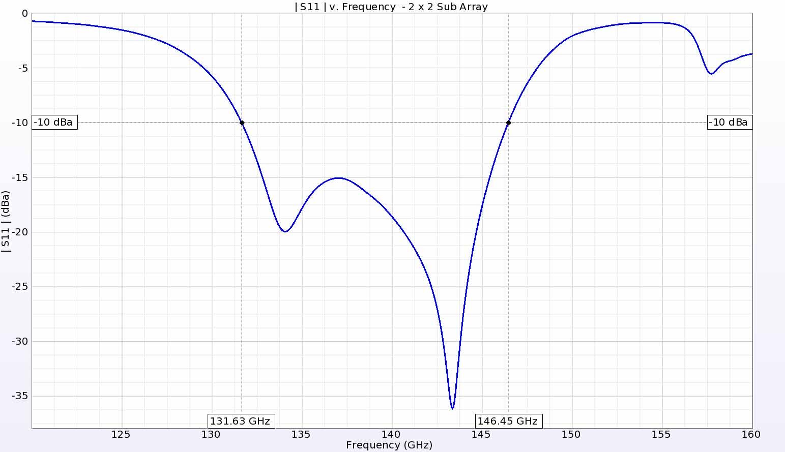
Figure 5: The return loss for a single 2x2 antenna element shows good performance below -10 dB from about 132 GHz to 146 GHz.
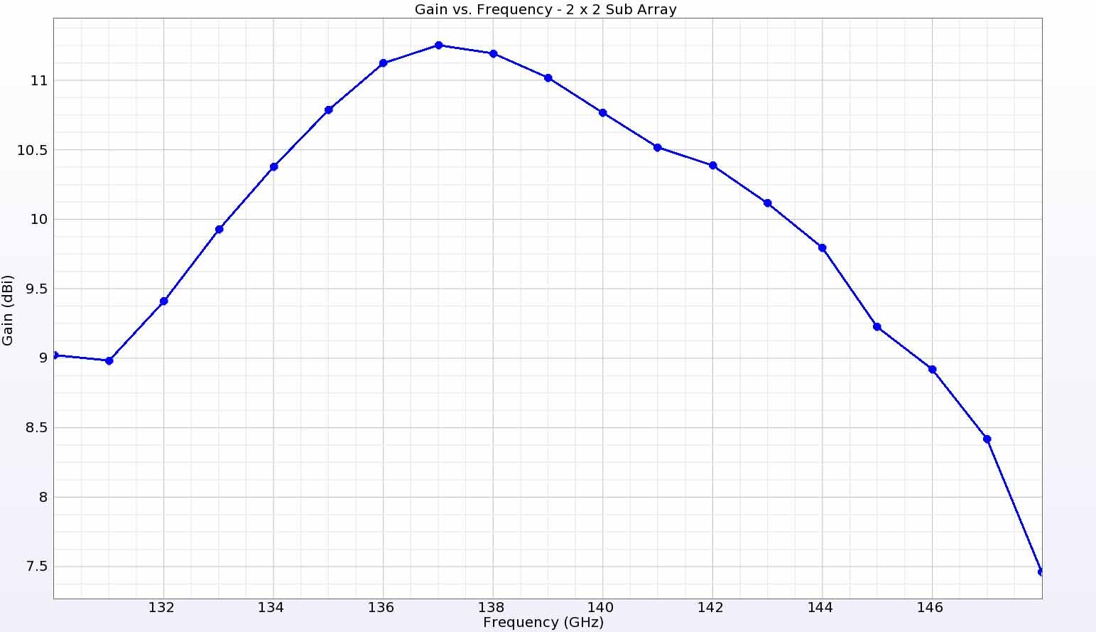
Figure 6: The gain versus frequency is plotted at a point directly above the antenna element and shows gain ranging from 9 dBi at the edges to a peak of 11.5 dBi in the center of the frequency range.
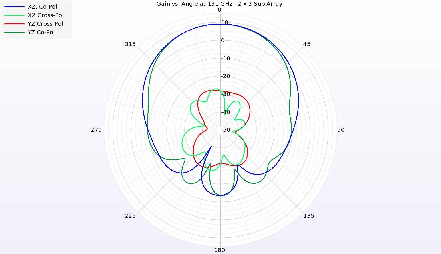
Figure 7: At 131 GHz, the antenna element has similar co-pol gain in the two principal planes. The cross-polarized radiation is significantly reduced.
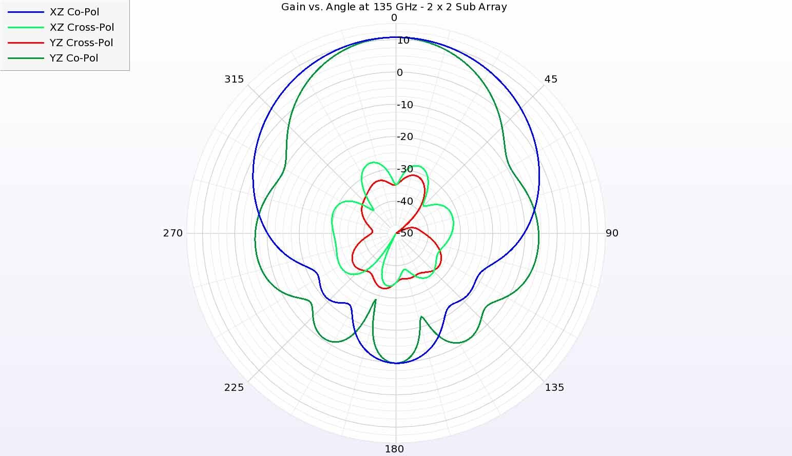
Figure 8: The antenna gain in the principal planes at 135 GHz shows similar performance with a slight narrowing in the YZ plane compared to the XZ plane.
To form the array, a primary H-junction power divider is designed with a single input port from the source in the center and four output ports which will each feed a secondary H-junction with antenna elements. The primary H-junction constructed in SIW is shown in Figure 11. When simulated with waveguide ports on each of the input and output locations, the return loss is found to be below -10 dB over a frequency range from 120 to 150 GHz, as shown in Figure 12. The secondary H-junction, shown in Figure 13, has an input port at the lower center and four output ports that will each attach to an antenna element like the one shown in Figure 1. As shown in Figure 14, the return loss of the secondary H-junction is also below -10 dB for the entire frequency range from 120 to 150 GHz.
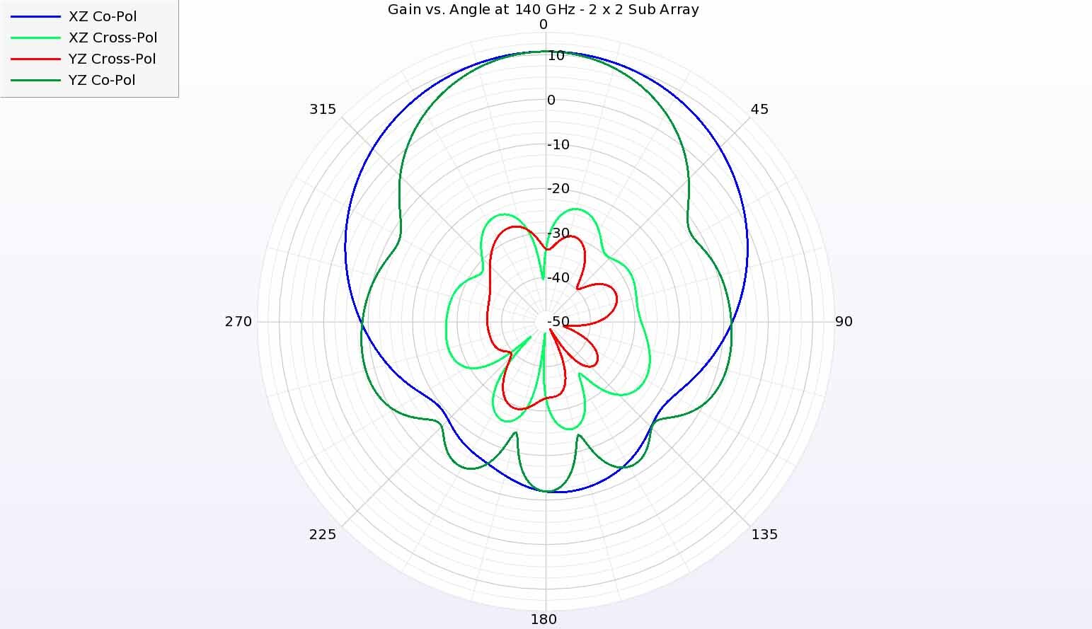
Figure 9: At 140 GHz, the antenna gain patterns show similar performance in the two principal planes with slightly broader beamwidth in the XZ plane.
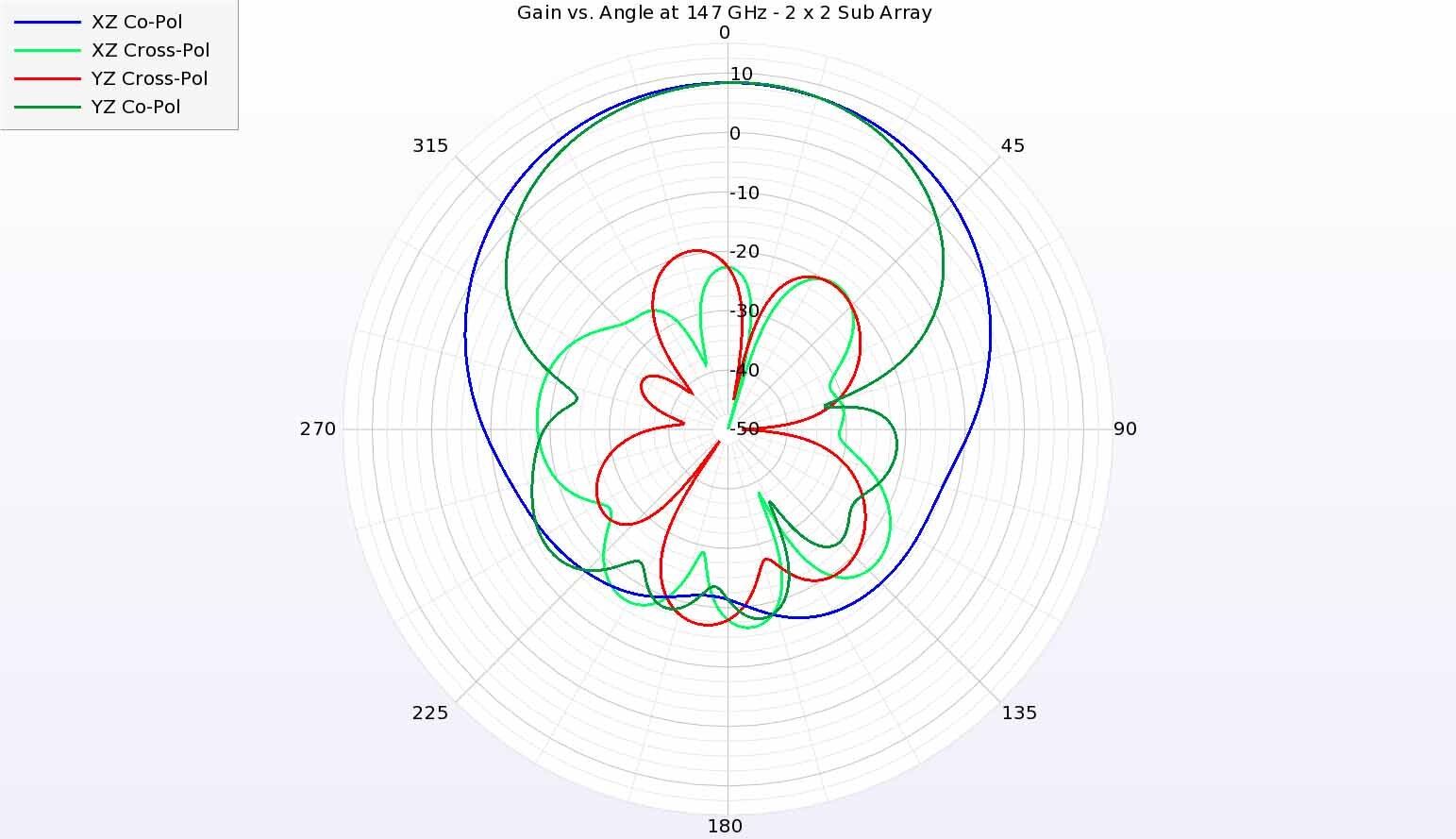
Figure 10: At 147 GHz, the antenna gain patterns still have similar gain as the lower frequencies, but the gain in the YZ plane is not as broad as in the XZ plane and the cross-polarized gain is growing to higher levels.
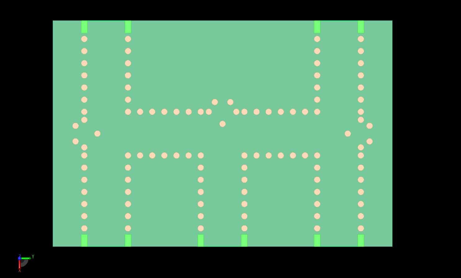
Figure 11: The primary H-junction that distributes the input signal from the source to the four secondary H-junctions is shown with the input port at the center bottom and the four output ports in the corners.
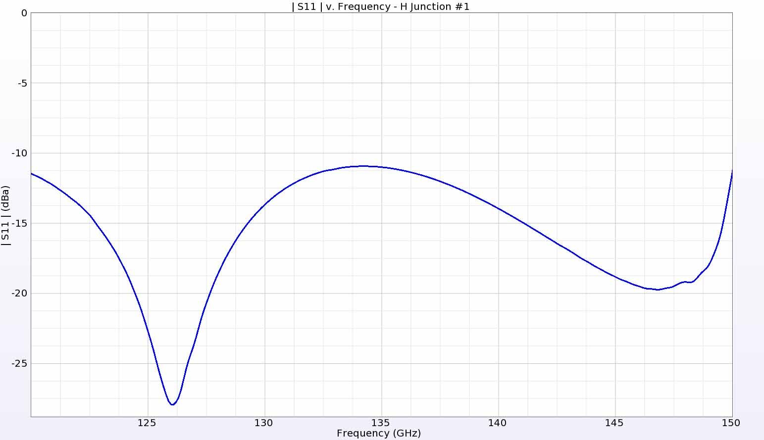
Figure 12: The return loss for the primary H-junction has good performance over the entire frequency range of interest.
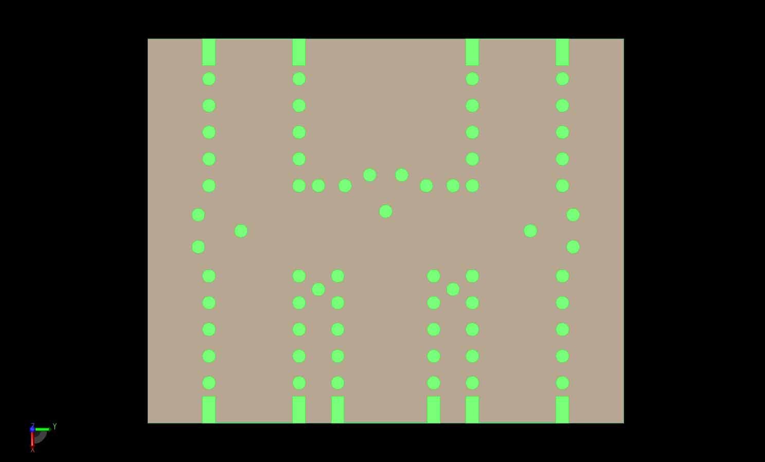
Figure 13: The secondary H-junction divides the input signal from the primary H-junction and spreads it to the four antenna elements. The input port is located in the center bottom of the junction while the output ports are in the four corners.
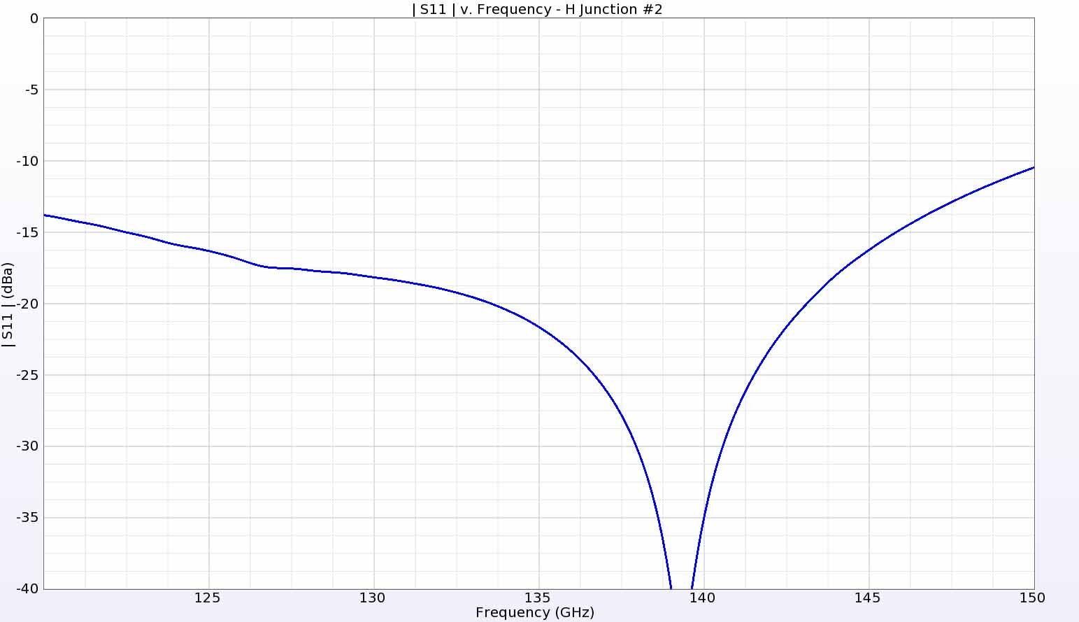
Figure 14: The return loss for the secondary H-junction has good performance over the entire frequency range of interest, similar to the primary H-junction.
The final 8x8 array is assembled by attaching four of the secondary H-junctions to the primary H-junction output ports, as shown in Figure 15. On each of the four output ports of each secondary H-junction, an antenna element is positioned. The final structure is placed on a larger ground plane that measures 25 x 10 x 0.616 mm with the array positioned at one end and a waveguide feed port attached to an SIW line that connects to the primary H-junction input port. The resulting structure is shown in Figure 16 and a top-down view of the array elements is shown in Figure 17.
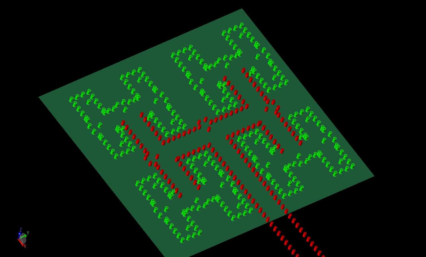
Figure 15: The full power divider layer is shown with the input signal coming from the bottom and feeding the primary H-junction with the red vias. The four secondary H-junctions are visible with the light green vias. Each secondary H-junction will connect to four antenna elements.
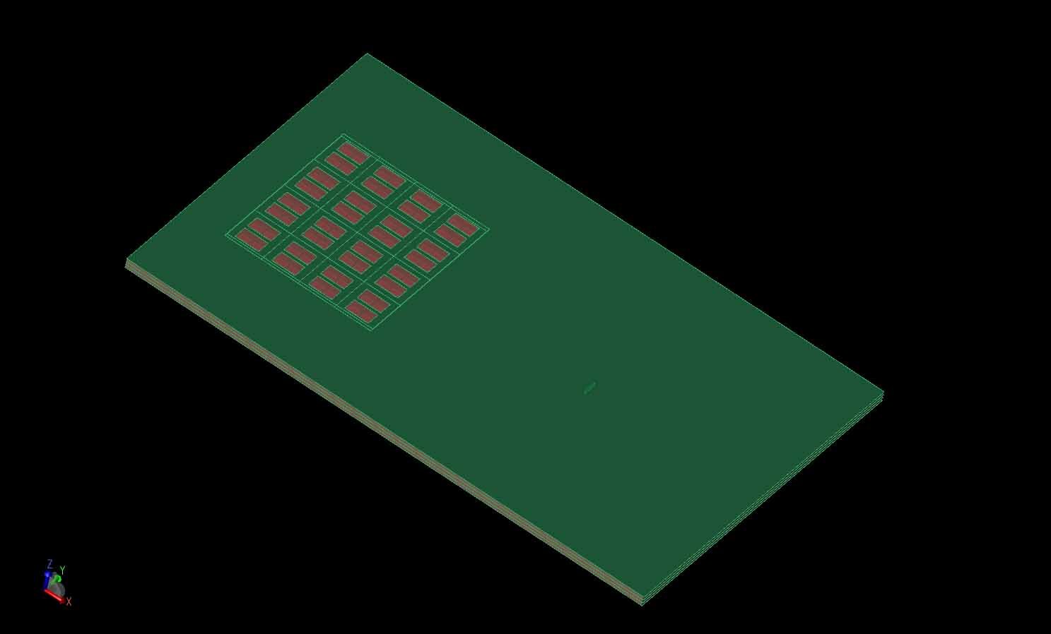
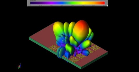
Figure 16: The full antenna array structure is shown with the 8x8 elements visible at the top of a 25x10 mm layered sheet.
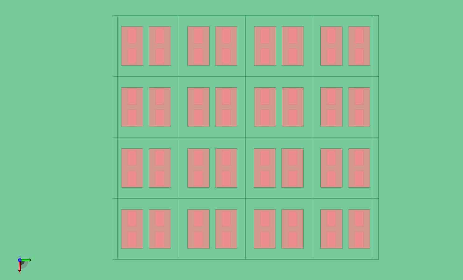
Figure 17: A top-down view of the 8x8 antenna elements is shown.
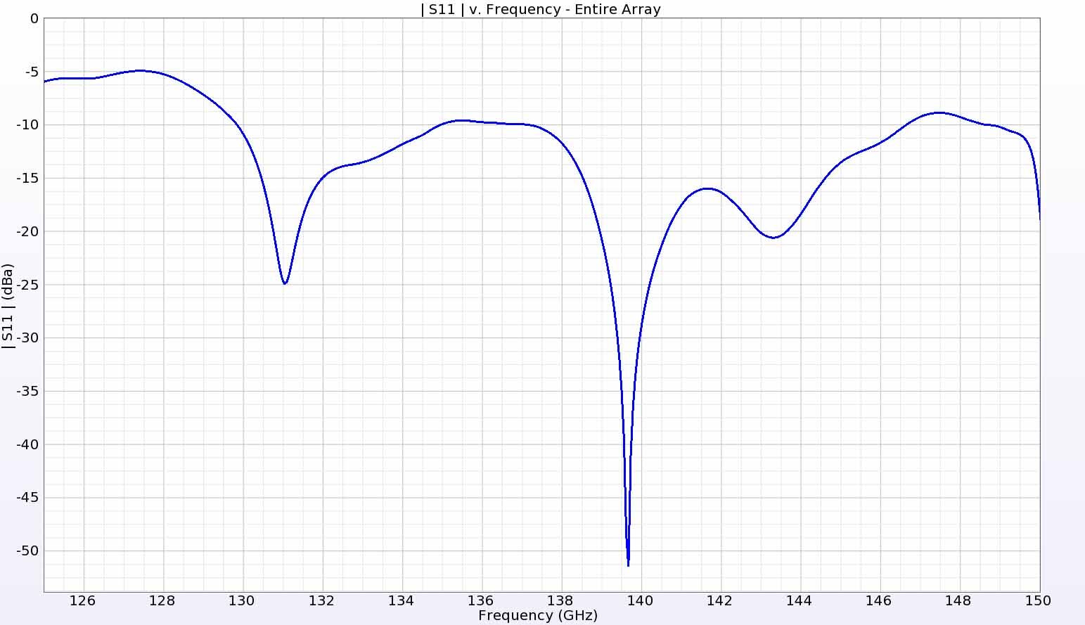
Figure 18: The return loss for the entire array is mostly below -10 dB from 130 to 146 GHz.
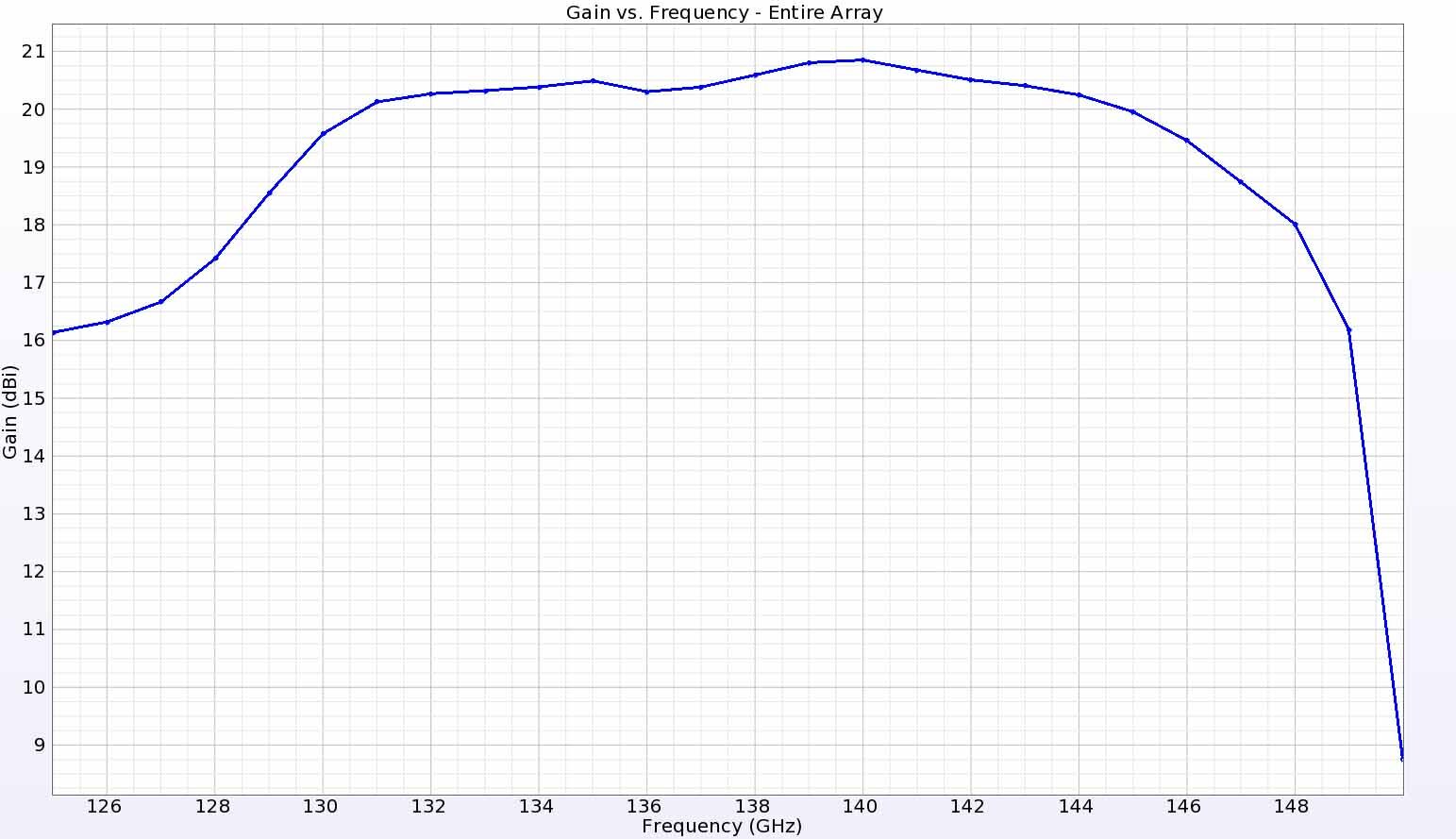
Figure 19: The gain of the array at a point directly above is smoothly varying from 17.5 dBi on the edges to a peak of 21 dBi at 140 GHz.
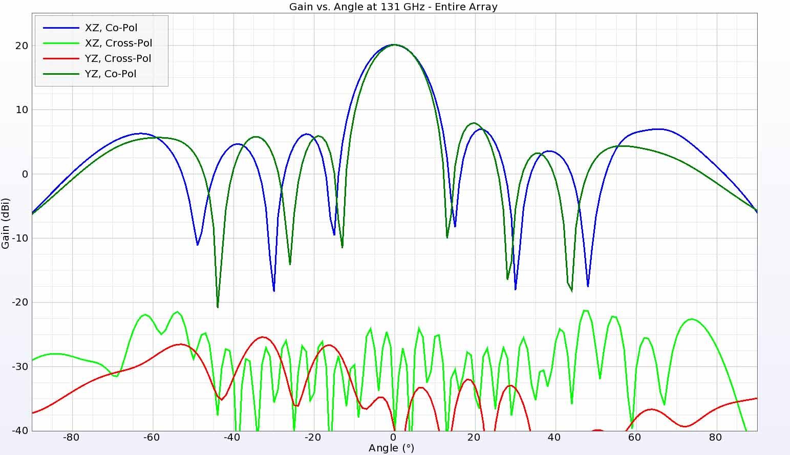
Figure 20: The gain patterns in the principal planes at 131 GHz show similar shape with sidelobes below 10 dB down from the peak and low cross-polarized gain.
The return loss for the entire structure is around -10 dB for a bandwidth of 130 GHz to 146 GHz as shown in the plot in Figure 18. The gain above the array is found to vary between about 19.5 dBi at the end points of 130 GHz and 146 GHz to a peak of nearly 21 dBi at 140 GHz. In the principal planes, the gain pattern is found to have a peak at 0 degrees with side lobes at least 10 dB below the peak. The gain pattern plots for 131 GHz, 135 GHz, 140 GHz, and 144 GHz are shown in Figure 20, Figure 21, Figure 22, and Figure 23, respectively. Three dimensional views of the gain patterns at the same frequencies are shown in Figure 24, Figure 25, Figure 26, and Figure 27, where the pattern shape and gain level are fairly similar, showing little variation in the array performance with frequency. In Figure 28 the efficiency of the array is plotted with values around 60% for the entire frequency range.
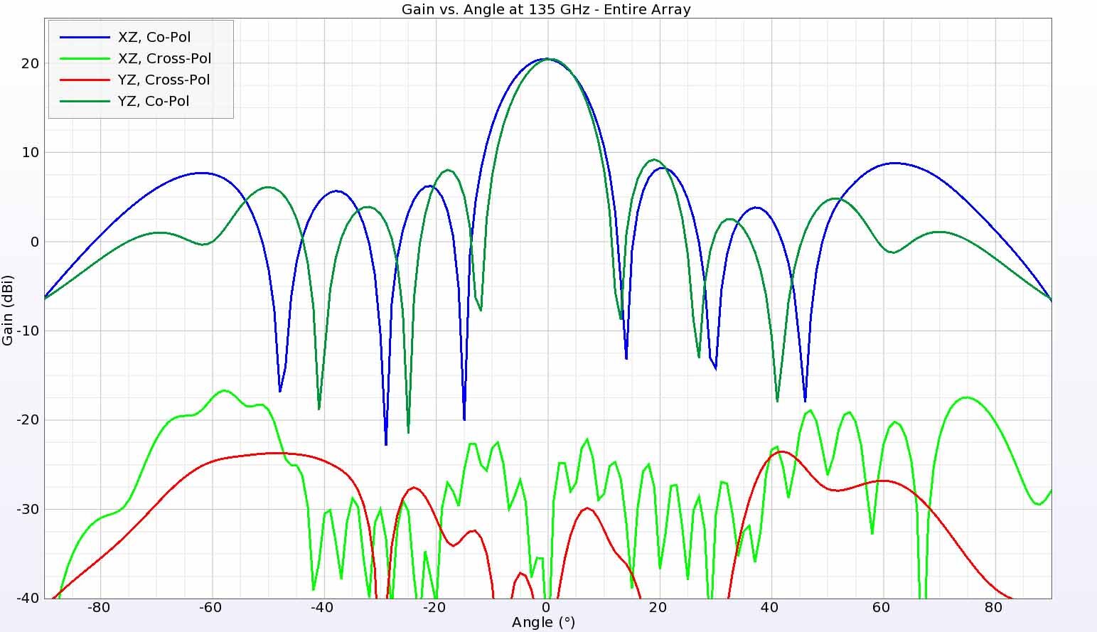
Figure 21: The gain patterns at 135 GHz show similar behavior to those at 131 GHz.
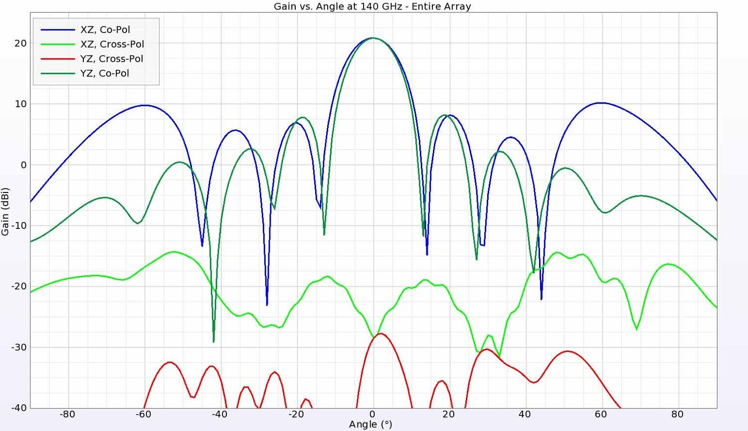
Figure 22: At 140 GHz the sidelobes get slightly larger but remain at least 10 dB down from the peak.
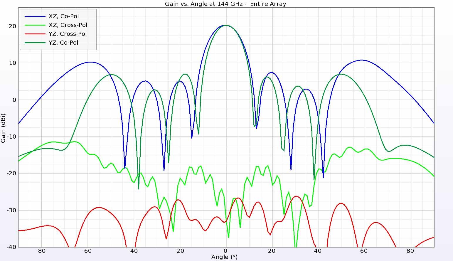
Figure 23: At the top of the frequency range at 144 GHz, the gain patterns remain very similar to those at the other frequencies.
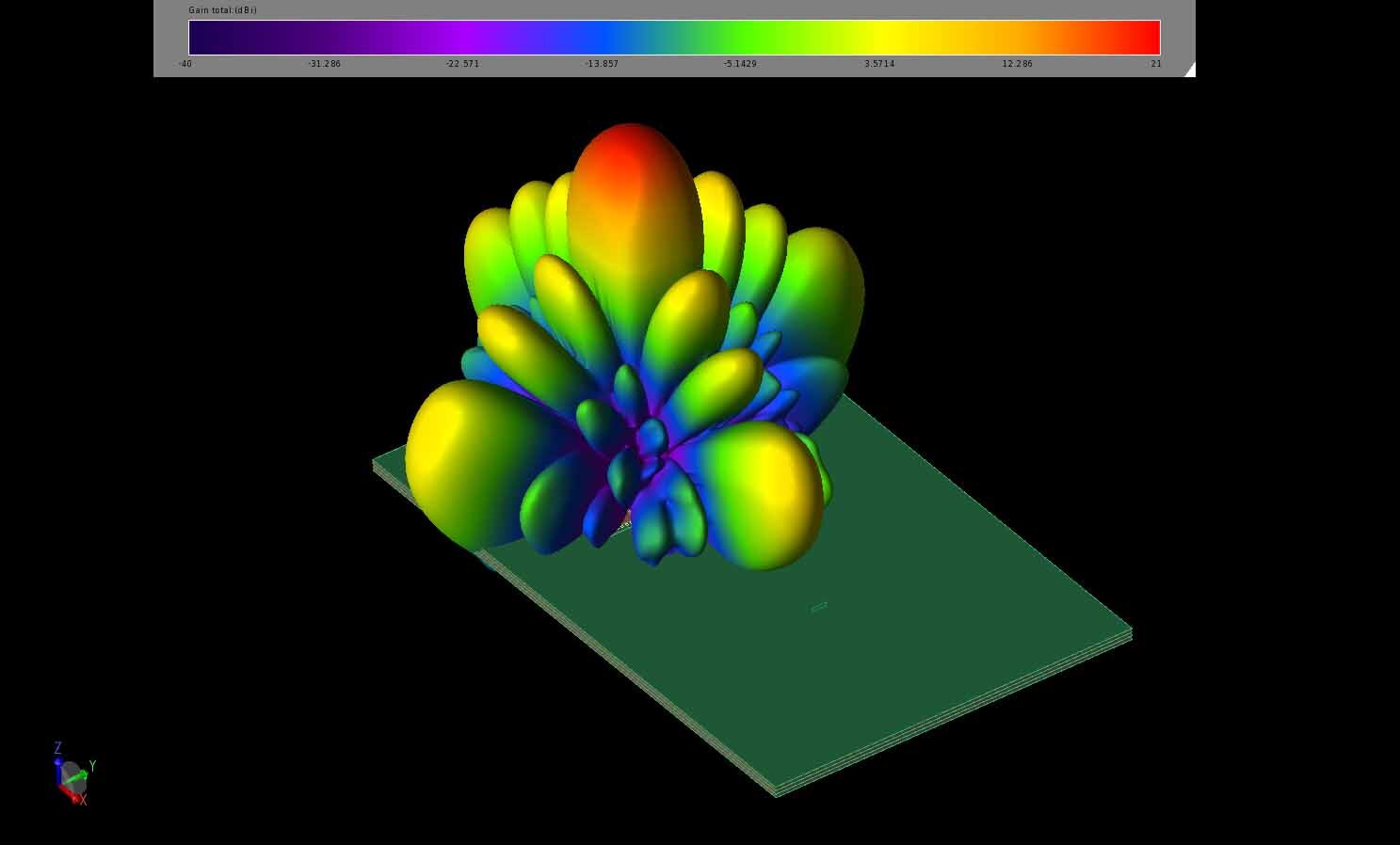
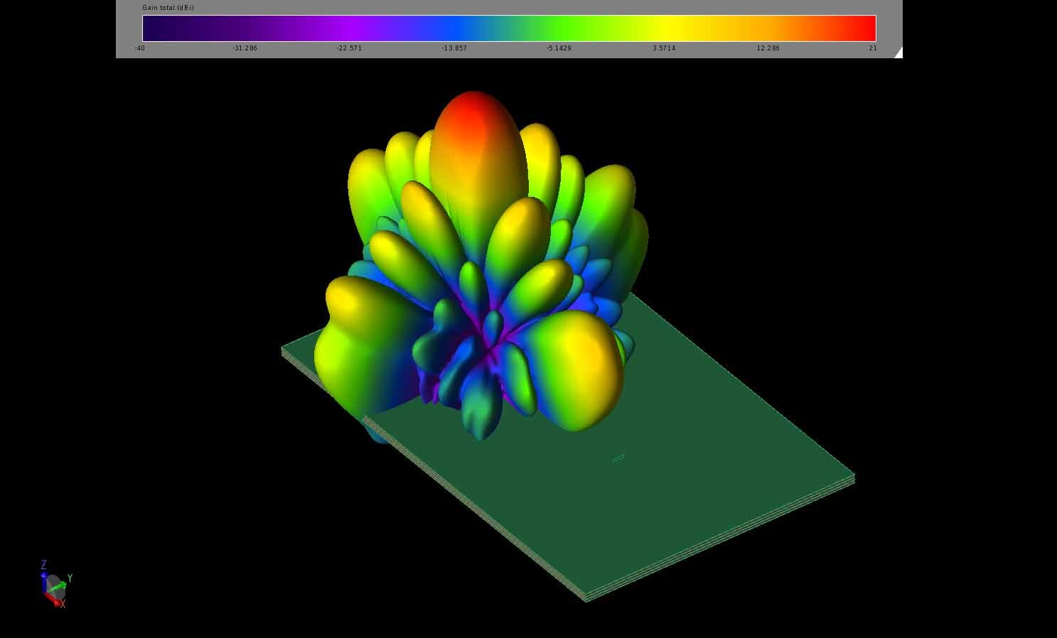
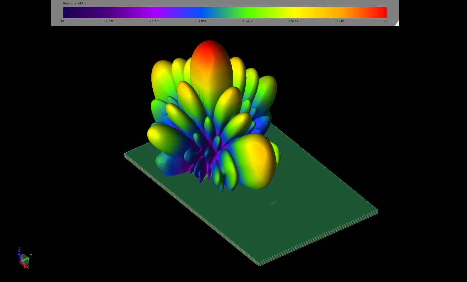
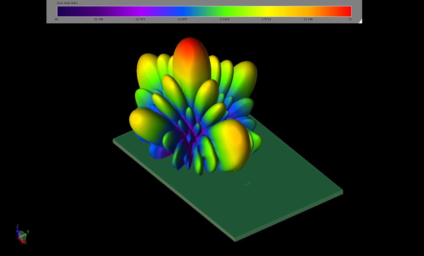
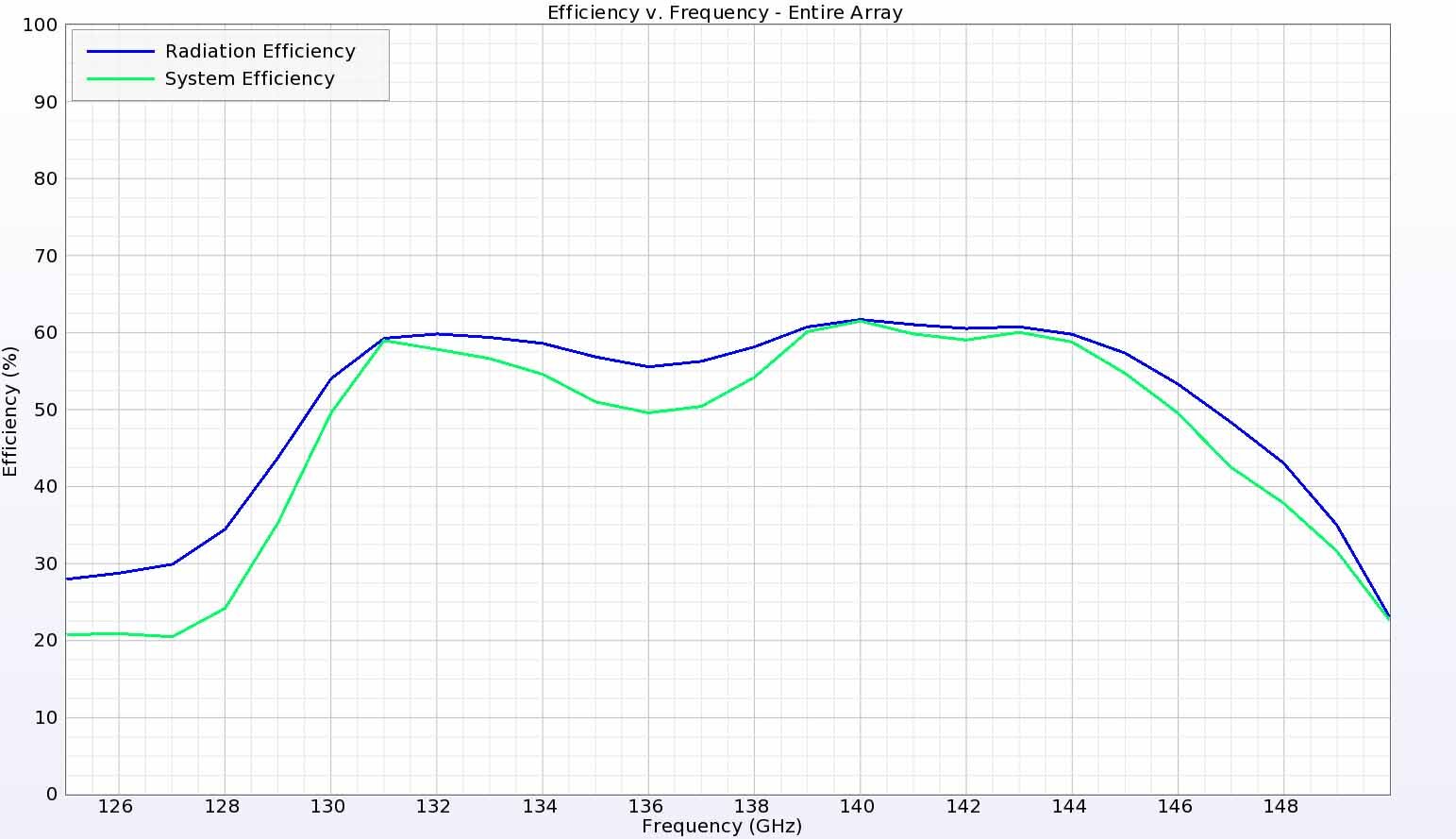
Figure 28: The efficiency of the antenna array is about 60% over the entire frequency range of interest.
Conclusion
This example demonstrates the performance of an 8x8 antenna array at 140 GHz that is constructed with multiple substrate-integrated cavities. The array has little variation in the gain pattern shape and levels over a broad frequency range. This antenna array could be useful for wireless communications in future 6G applications.
Reference
J. Xiao, X. Li, Z. Qi and H. Zhu, "140-GHz TE340 -Mode Substrate Integrated Cavities-Fed Slot Antenna Array in LTCC," in IEEE Access, vol. 7, pp. 26307-26313, 2019, doi: 10.1109/ACCESS.2019.2900989.